The Initiative has successfully released EPAC1.0 Test Chip for fabrication
The European Processor Initiative (EPI) https://www.european-processor-initiative.eu/, a project with 28 partners from 10 European countries, with the goal of helping the EU achieve independence in HPC chip technologies and HPC infrastructure, is proud to announce that we have successfully released our EPAC1.0 Test Chip for fabrication.
One key segment of EPI activities is to develop and demonstrate fully European-grown processor IPs based on the RISC-V Instruction Set Architecture, providing power-efficient and high-throughput accelerator cores named EPAC (European Processor Accelerators). Using the RISC-V Instruction Set Architecture will allow leveraging open-source resources at hardware architecture and software level, as well as ensure independence from non-European patented computing technologies.
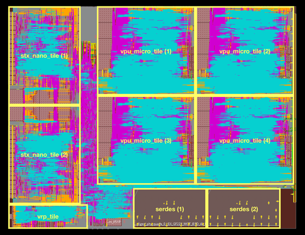
EPAC combines several accelerator technologies specialized for different application areas. The test chip, shown in figure 1 below, contains four vector processing micro-tiles (VPU) composed of an Avispado RISC-V core designed by SemiDynamics and a vector processing unit designed by Barcelona Supercomputing Center and the University of Zagreb. Each tile also contains a Home Node and L2 cache, designed respectively by Chalmers and FORTH, that provide a coherent view of the memory subsystem. The Stencil and Tensor accelerator (STX) was designed by Fraunhofer IIS, ITWM and ETH Zürich, and the variable precision processor (VRP) by CEA LIST. These specialized accelerators are connected with very high-speed network on chip and SERDES technology from EXTOLL.
The EPAC design was finalized by Fraunhofer IIS for chip integration in GLOBALFOUNDRIES 22FDX low-power technology and will be integrated and evaluated in the FPGA-based board designed by FORTH, E4 and the University of Zagreb. The successful fabrication of EPAC will showcase the next step in accelerator-based green HPC computing.
The outlook
The next generation of the EPAC accelerators and interfaces will be improved and refined for even higher performance and lower power levels in 12 nm technologies and below, and by adding a chiplet approach.
Jesus Labarta, BSC (EPAC Coordinator): I am really happy how partners with different backgrounds and motivations have been able to collaboratively develop this chip, putting all their efforts towards a collective success. It is a fully European design, driven by a vision of throughput-oriented computing and featuring characteristic that will result in high programmer productivity and achieve very high performance at low power and cost. Although just an initial Test Chip, it can be a significant step forward in HPC but also for edge and embedded applications.
Norbert Schuhmann, Fraunhofer IIS: The key challenge in this design and architecture was not only to achieve highest throughput and low power levels within the accelerators running on more than 1 GHz, but also to be in sync like in a concerto with memory accesses and data transport inside the chip and to the peripherals at rates above 200 Gbit/s.


