Accelerator Processor Stream

Stream 3 of the EPI SGA2 project builds on the achievements of the first phase, EPI SGA1, to demonstrate a completely European IPs based on the RISC-V Instruction Set Architecture. This first phase provided the basis for the development and provision of tangible hardware and software and sets the path toward EU HPC technology, where SGA2 steps in to improve and deliver a seamless heterogeneous accelerator based on the EPAC architecture.

EPAC architecture includes RISC-V vector tiles (VTILE), specialized Deep Learning and Stencil accelerators (STX), and variable floating point precision cores (VRP) all carefully engineered in a heterogeneous tile architecture whose subunits comply to the RISC-V standardization efforts.


Figure 1 EPAC1.0 Test Chip in GF22 Technology

EPI SGA1 resulted with the test chip of the first version of EPAC architecture implementation (EPAC1.0) in the GF22 technology and consisting of the following subunits (tiles):

  • Four RISC-V Vector (RVV) tiles composed of the scalar, two-way in order Avispado core and 8-lane Vector Processing Unit (VPU) implementing v0.7 of RISC-V Vector extension ISA.
  • Two STX tiles consisting of Stencil/Tensor Accelerator cores,
  • One VRP tile consisting of Variable floating point precision core.

Software Development Vehicles (SDVs) provided for early application porting and analysis, include Vehave, the software emulator of the RISC-V and Vector ISA, and an FPGA implementation of the RTL design that proved extremely useful for verification of the hardware and the system software including a vectorising compiler and a Linux kernel. Besides being usable as an accelerator for a general-purpose host, Avispado RISC-V core with vector extensions is a self-hosted general purpose HPC node running Linux. Another important component developed under SGA1 is the additions for RISC-V Vector extensions into the Compiler explorer – an open-source web application for interactive code generation and observations. Continuous integration system based on the FPGA implementation was very useful to identify and verify fixes and co-design improvements for the next versions of the chip that will be done in SGA2.

Continuing the developments from SGA1, SGA2 aims to produce a new EPAC1.5 test chip which will include improvements and fixes realized through the employed co-design methodology based on the SDV described previously. By the end of SGA2, the consortium will deliver the second test chip EPAC2.0 with additional features such as support for v1.0 of RISC-V Vector Extensions, improved microarchitecture features such as branch prediction, new data types, out-of-order execution, and interface to the VPU. New VPU will include more FPU units per tile.  Moreover, EPaC2.0 will feature improved cache management policies, support of very large number of outstanding memory requests, on chip memory controller, inclusion of memory compression capabilities, improved NoC, chip to chip connectivity and PCIe. And all of that migrated to GF12 technology. System software infrastructure (compiler, runtimes, libraries and operating system) will be upgraded and maintained.

SGA2 will also extend the SDV environment and provide improved framework for partners and external users willing to gain the head start and experience in preparing their codebase for high-throughput processor with vector extensions based on EPAC architecture. Remaining tiles will complement the EPAC in specific computation kernels from stencil/deep learning and approximate computing domains. The SGA2 work on the STX will, beyond general improvements, address challenges identified in SGA1 such as a focus on sparse access patterns, mixed precision and new number formats including POSIT.

Besides the continuation of activities from SGA1, SGA2 stream 3 will also include efforts to integrate other specialized cores or potential accelerator technologies such as the Kalray processor and the Menta FPGA devices under the EPAC RISC-V framework. Building on top of SGA1 and coordinating its activities with the EU Pilot project, SGA2 will contribute to demonstrate how it is possible to have a very cost-effective EU independent technology for the HPC and other domains.

RVV: RISC-V Vector Tile

RVV vector tile consists of the general-purpose, 64-bit RISC-V core Avispado, developed by Semydynamics. Avispado, tightly coupled with the vector processing unit Vitruvius, developed by BSC and the University of Zagreb. The interface is realized using, purpose-built Open Vector Interface 1.0 specification. The RVV tile also contains physically distributed, logically-shared 256KB L2 cache developed by Chalmers/Forth. The Tile is connected in a coherent fashion to other tiles using a custom CHI.B Mesh interconnect developed by Extoll. Although the test chip only contains 4 vector tiles, the architecture is highly scalable and allows for up to 512 tiles to be aggregated coherently together using a scalable mesh architecture.

Figure 2 EPAC1.0 RVV Vector tile die consisting of Avispado RV-64 (CORE), Vitrivius vector processing core (VPU) and L2 cache/HN node interface

Avispado core implements RV64GCV ISA and features OVI interface for connecting VPU units and extending the core with the support for vector instructions. The core also supports compressed instructions, SV48 virtual memory and unaligned instructions.  Block diagram of the Avispado core with Vector Unit is shown below.

Figure 3 Avispado RISC-V core with Vector Unit

Avispado sends arithmetic vector instructions to the vector unit through the Vector-FP-Issue-Queue (VFIQ). Vector memory instructions (vector loads and stores) are processed in Avispado itself, through the Memory-Issue-Queue (MIQ) and the vector address generation unit (vAGU). Vector memory addresses are translated to a physical address according to SV48/39, checked against the PMA and lookup the Data cache to guarantee coherency between vector and scalar accesses. If the data is not found in the cache, a CHI request is made to the NOC. Upon data return, 512b are delivered to the vector unit per clock cycle.

The Vector Unit or VPU communicates Avispado core through the Open-Vector Interface (OVI). It currently implements version 0.7.1 of the RISC-V V-extension featuring a maximum vector length (VL) of 256 double-precision (64-bit) elements (16384 bits). It supports register renaming by implementing 40 physical vector registers whose elements are distributed among the set of parallel identical vector lanes, which communicate through a unidirectional ring. The VPU provides a lightweight out-of-order execution mechanism by splitting arithmetic and memory operations into two concurrent instruction queues, allowing overlapped execution. The VPU is completely configurable, although the baseline design in the EPAC test chip implements eight vector lanes interconnected through a unidirectional area-efficient ring. The detailed block diagram of the VPU is shown below.

STX: Stencil/Tensor Accelerator Tile

An important aspect of EPI (both, SGA1 and SGA2) has been the consideration of heterogeneous acceleration to achieve even higher energy efficiency for domain specific applications. Consequently, specialized blocks for deep learning (DL) and stencil acceleration have been an important part of the EPI roadmap. The capabilities brought out with these specialized accelerators will address workloads in HPC centres for stencil computations, while the DL block will target learning acceleration as part of the acceleration stream motivated by “optimised performance and energy efficiency” for “specialised computations”. At the beginning of SGA1, two different domain-specific accelerators for DL and stencil computations were suggested. During the first few months of the project, researchers from Fraunhofer Institute, ETH Zürich and the University of Bologna were able to merge the functionality of both units into a very efficient computation engine that has been named STX (stencil/tensor accelerator) with an optional add-on called SPU (Stencil Processing Unit) to enhance the cluster for Stencil loads.

The main goal of STX is to achieve a significantly higher (at least 5x-10x) energy efficiency over general purpose/vector units. The efficiency tells us how many computations can be performed with the unit, and the early target for the STX unit was to achieve at least 5x more energy efficiency (TFLOPS/W) than the vector unit on deep learning applications. In the first few months of the project, it became clear that these estimations are rather conservative, and the effective efficiency within EPI chips will be significantly higher. For applications that require only inference using quantized networks, this efficiency will be another 10x higher.

STX has been designed around a novel RISC-V core named Snitch. This is a small and efficient 32-bit RISC-V core which is supported by a capable 64-bit FPU with SIMD support. The Snitch core has been enhanced with hardware supported loops for floating point operations (FREP) and streaming semantic registers (SSR) that allow the FPU to independently fetch and write back using a wide range of regular data access patterns. A typical instantiation of STX uses 8 such Snitch cores for computation and a further Snitch core with DMA enhancements to help with data movement to and from the cluster. The system can also be enhanced by the SPU unit which contains a VLIW architecture optimized for Stencil workloads. The SPU targets extreme efficiency and easy programmability for kernels with static access patterns and only local data dependencies. Typical applications are finite-difference solvers. However, dense arithmetics and FFTs are a primary target. The SPUs are developed in a strict hardware software co-design approach which includes users, application and toolchain developers as well as hardware architects and engineers. This way the SPU equipped STX achieves more than 70% of the possible peak floating-point throughput of real world scientific kernels without SPU specific code modifications.

STX has been designed as a modular building block with several parametrization options. Each STX accelerator consists of several clusters of computing units, a typical instance would have four of such clusters. Each cluster in turn consists of 4-16 compute Snitch RISC-V cores (typically 8), one specialized Snitch RISC-V core for orchestrating data transfers as well as, 0 – 4 SPU units. All these units access a local scratchpad memory or TCDM (64 – 256kB), which will be filled using the specialized DMA unit. In theory, a 4 cluster system with 8 compute cores running at 1GHz clock speed can perform 64 DP GFlops/s. Practical experiments have shown that for common machine learning tasks, an FPU utilization of over 85% can be achieved. Multiple instances of STX can be instantiated in an EPAC tile.

STX is programmed using OpenMP, there are solutions that allow regular operations to be offloaded to the STX unit from an ARM system (in the GPP) or the 64-bit RISC-V core (in the EPAC tile) using both GCC and LLVM based flows that continue to be developed further as part of the EPI project.

VRP: Variable Precision Tile

The VRP Tile enables efficient computation in scientific domains with extensive use of iterative linear algebra kernels, such as physics and chemistry. Augmenting accuracy inside the kernel reduces rounding errors and therefore improves computation’s stability. Contemporary solutions for this problem have a very high impact in memory and computation time (e.g. use double precision in the intermediate calculations), thus validating the motivation for specialized hardware acceleration.

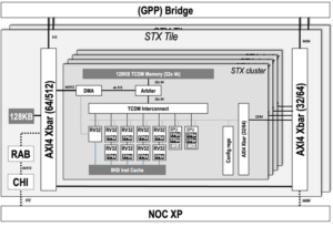
The hardware support of variable precision, byte-aligned data format for intermediate data optimizes both memory usage and computing efficiency. When the standard precision unit cannot reach the expected accuracy, the variable precision unit takes the relay and continues with gradually augmenting precision until the tolerance error constraint is met. The offloading from the host processor, i.e. General Purpose Processor or GPP in EPI, to the VRP unit is ensured with zero-copy handover thanks to IO-coherency between EPAC and GPP.

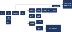
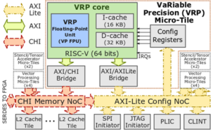
The VRP accelerator is embedded as a functional unit in a 64-bits RISC-V processor pipeline. The unit extends the standard RISC-V Instruction set with hardwired arithmetic basic operations in variable precision for scalars: add, subtract, multiply and type conversions. It implements other additional specific instructions for comparisons, type conversion and memory accesses. The representation of data in memory is compliant with the IEEE 754-2008 extendable format, which eases the integration with the GPP. The unit features a dedicated register file for storing up to 32 scalars with up to 512 bits of mantissa precision. Its architecture is pipelined for performance, and it has an internal parallelism of 64-bits. Thus, internal operations with higher precision multiple of 64 bits are executed by iterating on the existing hardware. The VRP micro-tile also features a high-throughput memory unit (load store unit and data cache) with a hardware prefetching mechanism, that hides the access latency to memory when running commonly memory-bound scientific applications.

The VRP programming model is meant for smooth integration with legacy scientific libraries such as BLAS, MAGMA and linear solver libraries. The integration in the host memory hierarchy is transparent for avoiding the need of data copy, and the accelerator offers standard support of C programs. The libraries are organised in order to expose the variable precision kernels as compatible replacements of their usual counterparts in the BLAS and solver libraries. The complexity of arithmetic operations is confined as much as possible within the lower level library routines (BLAS). Consistently, the explicit control of precision is exclusively handled at solver level.

EPI Programmable Logic based Accelerator

Systems designers have to use a multi-chip approach so as to end up with both hardwired acceleration of some tasks and reconfigurable implementation of some others. US-based, Xilinx-AMD has announced its Versal platform which will include hardwired accelerators and reconfigurable logic but their chips are mainly targeted to the cloud market so far. Heterogeneous SoCs and platforms integrating manycore CPUs, hardware accelerators, and reconfigurable programmable logic enables:

  • HW/SW co-Design and co-development tools, aimed at accurate design space exploration at the early stages of the design and fast and efficient designing and programming of such heterogeneous platforms
  • Complete software stacks from application programming to AI-libraries, to runtime systems, to operating Systems which will take full advantage of the features of such heterogeneous devices
  • The implemented complete systems, including both the Hardware and the software, satisfy

hard real-time, safety and security requirements

In HPC applications, reconfigurable programmable Logic is mainly usefull on support functions that are on critical path and that are requiring reconfigurable feature in the field. In general, such hardware capability is acting as a Common Plateform Accelerator enabling:

  • Acceleration of specific tasks for datacenter services boosting ML & AI performance
  • To offload a wide variety of small tasks from CPU and speed process along
  • To handle atypical data types, specifically FP16 (or half-precision) values used to speed up AI training and inference

Thus, SGA2 will also provide a European field programmable gate array accelerator developed by Menta in the fifth architecture generation. Applications such like cryptography, AI, CPU support functions such as task scheduling or adaptive variable precision units will be implemented on programmable logic core from Menta. Such solution provides hardware flexibility to the overall system and will enable the HW/SW co-Design architecture concept in SGA2. It will be a powerful accelerator for HPC with applications such as that will also allow evolving

The technology will be supported by Menta’s unique eFPGA configuration software: Origami Programmer, which is allowing to program the accelerator core and generates the new bitstreams, in the field.


Menta eFPGA IP V5: EPI programmable logic accelerator core

Load More
Our website uses cookies to give you the most optimal experience online by: measuring our audience, understanding how our webpages are viewed and improving consequently the way our website works, providing you with relevant and personalized marketing content. You have full control over what you want to activate. You can accept the cookies by clicking on the “Accept all cookies” button or customize your choices by selecting the cookies you want to activate. You can also decline all cookies by clicking on the “Decline all cookies” button. Please find more information on our use of cookies and how to withdraw at any time your consent on our privacy policy.
Accept all cookies
Decline all cookies
Privacy Policy