- The European Processor Initiative (EPI) has successfully completed its first three-year phase, delivering cutting-edge technologies for European sovereignty on time and within a limited budget, despite the constraints of the COVID-19 pandemic
- Highlights include the Rhea general-purpose processor, EPI accelerator proof of concept and embedded high-performance microcontroller for automotive applications
- The successful completion of this phase, SGA1, paves the way for the second instalment of the project, which kicks off in January 2022
The European Processor Initiative (EPI), a project with 28 partners from 10 European countries aiming to make the EU achieve independence in high-performance computing (HPC) chip technologies and infrastructure, is proud to present key results achieved in phase one (2018-2021).
These results stem from three major research and innovation domains, the General-Purpose Processor (GPP), Accelerator (EPAC) and Automotive streams, complemented by a number of common activities.
General-Purpose Processor (GPP)
Atos, a global leader in digital transformation, cybersecurity, cloud and HPC, is the lead partner of the General-Purpose Processor (GPP) stream. Together with SiPearl, the company bringing to market the high-performance and low-power European processor, and other EPI partners, they defined the architectural specifications of Rhea, the first generation of the EPI General-Purpose Processor (GPP) implementation and its future derivates.
With 29 RISC-V cores, the Arm Neoverse V1 architecture used by SiPearl to design Rhea will offer an effective, scalable and customisable solution for HPC applications. Architectural decisions were taken following a co-design methodology and by analysing the performance of advanced intellectual property (IP) blocks. A scalable network-on-chip (NoC) to enable high-frequency, high-bandwidth data transfers between cores, accelerators, input / output (IO) and shared memory resources was also optimised by SiPearl.
To allow early software development and performance estimation of the EPI processor while the GPP was still at the implementation stage, a GPP virtual prototype was designed and used.
“We are proud of our success in designing a powerful GPP leveraging cutting edge technologies and IPs built and deployed exclusively by European universities and industrial leaders. We are confident that we will soon demonstrate the instrumental role of this GPP in enabling a European exascale computing machine, the next breakthrough in the HPC domain the world is expecting.” – said Stream Leader Emmanuel Ego (Atos).
“At SiPearl, we are very proud to bring to life the joint project of the European Processor Initiative. We worked hard through close collaboration with the initiative’s 28 partners – the scientific community, supercomputing centres, leading names from industry and innovative start-ups – who are our stakeholders, future users, and clients. With the release of the Rhea processor, we will all contribute to ensure European sovereignty in HPC applications such as personalised medicine, climate modelling, and energy management.” – said Philippe Notton, founder and CEO of SiPearl.
Rhea will integrate technologies by EPI partners and offers unique features in terms of memory architecture, memory bandwidth optimisation, security, and power management.
Memory
Memory controllers are one of the most critical IPs when it comes to GPP performance. To help evaluate architectural choices, CEA developed a complete simulation platform with specific instrumentations to analyse controller efficiency in driving the high-bandwidth HBM2E memories. The platform allows efficient analysis of the memory device interface thanks to the decoding and tracking of all memory commands and data. The HBM2E subsystem was simulated with multiple random and directive patterns targeting different traffic shapes and involving all the controller features in maintaining the HBM2E efficiency.
Security
A number of state-of-the-art embedded security features and key technologies were also designed in this stream. These include the standalone Security Management System (SMS) security IP developed by ProvenRun, providing advanced, common-criteria certified, sovereign security IP for HPC and edge processors.
To further bolster security, the University of Pisa contributed a set of crypto IPs, called “Crypto Tile”, integrated in the Rhea GPP by SiPearl. This provides a hardware security module with full security services for high-end symmetric (AES with 9 cipher modes), asymmetric (ECC, ECDSA, ECIES, ECDH) and hashing (SHA2/SHA3) cryptography, delivering several orders of magnitude of increased throughput and decreased energy cost as compared to a software solution.
The Crypto Tile also includes secure key storage and secure IP configuration, side-channel attack protection, on-chip true random number generation (TRNG), support of Linux kernel drivers, extreme key lengths for maximum security levels and high speed en(de)cryption throughput thanks to AXI4-based interface towards DMA and Arm or RISC-V programmable cores. Post-quantum cryptographic support is also provided thanks to real-time implementation of Lattice algorithms such as Crystals Kyber and Dilithium.
Power
Given the importance both of reducing the carbon footprint of future generation computing systems and enabling higher computation capabilities in post-Dennard scaling electronics, energy-efficient computing has been a key consideration in EPI from the outset. For this purpose, an open-source, RISC-V based power controller was designed by University of Bologna and ETH Zurich and integrated into the Rhea processor, harnessing advanced control and artificial intelligence (AI) algorithms for the power management of large-scale systems-on-chip (SoCs).
In addition, based on STMicroelectronics technology on power solutions, Atos and E4 Computer Engineering designed and manufactured the Voltage Regulator and Management reference platform to test the Board Management Controller (mapped inside a field-programmable gate array, or FPGA).
EPI GPP has achieved register transfer level (RTL) completion status as a result of the first phase of the EPI project. The Rhea full design implementation is currently at the validation stage using emulations.
The main result of general-purpose processor activities in EPI phase one, the Rhea processor, will be instrumental for the launch of European exascale supercomputers in 2023.
Accelerators
The EPI accelerator stream set out to deliver energy-efficient acceleration for HPC and AI workloads. With the European Processor Accelerator (EPAC) test chip proof of concept, EPI has demonstrated that it is possible to create an exclusively European design, while the use of open-source instruction-set architectures (ISAs) ensures freedom from proprietary licences and export restrictions.
This stream has fully embraced the open-source philosophy of give and take, contributing to the expansion of the RISC-V ecosystem and adding to the LLVM compiler database. The EPAC systems and FPGA software development vehicles make full use of the Linux operating system and contribute to the community with patches, device drivers, and additional functionality to popular open-source HPC software packages such as OpenMP and MPI. Furthermore, parts of the hardware such as the STX (stencil/tensor accelerator) were developed using a permissively licensed open-source approach around the PULP platform.
“The accelerator stream in EPI has emphatically proven that the RISC-V vector approach has the potential to transform the HPC sector, with designed-in-Europe architectures capable of delivering high performance on a low energy budget,” commented Stream Leader Jesús Labarta (Barcelona Supercomputing Center). “The work also epitomizes European traditions of open science and collaboration. Partners across Europe have joined forces to create something that no single organization could have achieved by itself. By working with open-source technologies and projects, the EPAC stream has helped expand the RISC-V ecosystem, making this technology viable for an increasing number of applications in the future.”
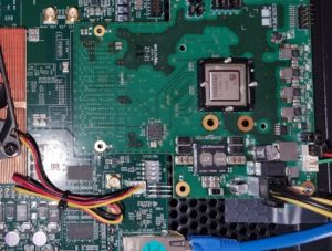
Figure 1 EPAC Test Chip on a test PCB
EPAC set out to provide a proof of concept for European-designed, RISC-V vector architectures for HPC acceleration. A suite of technologies has been developed to this end:
- The EPAC vector processing unit (VPU), design by BSC and UNIZG, shows the use of RISC-V long-vector architectures for high-performance computing is a viable approach, delivering high performance on a low energy budget, and that it can be scaled up in future.
- The vector unit is driven by Semidynamics’ vector-specialised Avispado RISC-V core and Gazzillion Misses™ technology for energy-efficient processing.
- The dedicated and flexible RISC-V based many-core stencil and tensor accelerator (STX), designed by ETH Zurich and Fraunhofer, leverages stencil processing units to offer exceptional energy efficiency and programmability for machine-learning and stencil workloads.
- Meanwhile, the variable precision accelerator (VRP), designed by CEA, enhances efficiency and reliability for scientific high-performance computing applications such as multiphysics simulations.
- The EPAC test chip also includes multiple distributed banks of shared L2 cache and coherence home nodes (L2HN) designed by FORTH and CHALMERS and optimised for the high-bandwidth requirements of the vector processing units while offering a coherent view of the memory system that facilitates multi-core programmability.
- All the processing units and the shared L2HN banks are connected via a high-speed NoC in a modular manner that permits the system to scale up. The test chip also includes advanced SERDES technology for very high-bandwidth off-chip and cross-chip communication. Both the NoC and SERDES were designed by Extoll.
- The PCB (daughter board) to enable the testing of the EPAC Test Chip was designed and developed by E4 Computer Engineering.
EPAC offers exceptional programmability, with generic codes being run successfully on the test chip with minimal modifications and a software development vehicle to support programmers. It is a genuine example of co-design, with a continuous integration system and rapid application of improvements in response to feedback.
Automotive
Coordinated by Infineon, a leader in automotive microcontrollers, the Automotive Stream has paved the way towards road-capable autonomous cars, thanks to the proof of concept for an innovative embedded high-performance compute (eHPC) platform and associated software development kit (SDK). This platform, in combination with a downsized, vehicle-tailored, general-purpose processor, meets the increasing demand for computing power in future cars in a cost-efficient, economically viable and functionally safe way.
“Overall, the achievements are evidence of collaboration, synergies and the team spirit which characterised the research work in the automotive stream”, – said Stream Leader Knut Hufeld (Infineon). “With its focus on cost-effective, safe and certified automotive solutions, it can be seen as a driving belt for the overall profitability of European processors in the field of HPC.”

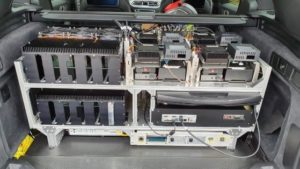
Figure 2: BMW X5 EPI Test Car and the EPI computing system in the rack.
The main achievement was demonstrated in a road-approved BMW X5 car to show the proof of concept for a pioneering eHPC Microcontroller Unit (eHPC MCU) which is integrated in a specially designed flexible modular computing platform (MCP) together with several EPI technology IPs. Numerous test drives were performed to collect data and evaluate test scenarios involving parameters of autonomous driving.
Among other features, the platform includes AI-supported integrated cameras and Elektrobit radar imaging analysis software, with integrated preparation for use of EPI accelerators in the system. It is the result of a close cooperation among the 16 partners in Stream4 aiming to fulfil its objectives of specifying a suitable eHPC Platform, define its architecture and develop the necessary software development kit (SDK).
Infineon also expanded the automotive microcontroller in terms of its architecture and performance ability so that it can act as master and control one or several accelerators. Relevant aspects were safety, security, fall back or redundancy for reduced application, with regard to the top Automotive Safety Integrity Level D (ASIL D) at system level, which is required for autonomous driving applications.
The platform is scalable and open for further technologies. The MCP has various slots for other technologies developed as part of EPI, including:
- future automotive versions of the EPI general purpose processor
- the EPAC RISC-V based accelerator
- the Kalray Massively Parallel Processor Array (MPPA®) accelerator tile for eHPC, developed as an IP in the Stream 2 and demonstrated for object detection using Kalray’s MPPA®-based Coolidge™ processor for final BMW automotive demonstration
- the Menta eFPGA
Test runs reveal that EPI now has specific technologies suitable for autonomous driving up to at least level 4 – where the vehicle drives independently most of the time – thus paving the way for the future.
In addition to the hardware platform, this stream also included the development of a complete software ecosystem, based to a large extent on software products by automotive software specialist Elektrobit. This area also comprises the automotive eHPC platform software stack, including the classic automotive open operating system architecture (AUTOSAR) development for Auto eHPC MCUs, and the adaptive AUTOSAR development for HPC GPPs and the L4Re hypervisor (virtualisation) that are crucial for automotive applications.
With regard to safety, a specific concept was jointly created for a software lockstep, thus contributing to an overall EPI safety concept.
After this three-year initial phase, the results and findings will be continued in further projects.
Common Activities
This stream acted as a provider for other technical streams. Excellent collaboration, both internally and with other streams, helped mitigate issues caused by pandemic-imposed travel restrictions and allowed the stream to meet its objectives, enumerated below.
This stream established a co-design process to shape the design of European processors. Simulations and models with different levels of detail and precision were created to identify the impact of design decisions on the performance of future applications. A benchmark suite of over 40 applications was used to support co-design and later evaluate the EPI processors. Applications have also been prepared to run on future EPI systems, by adapting and testing them on comparable hardware platforms and emulators.
The specification of a “common platform” architecture was defined and used as a backbone for architecture exploration, as the starting point for the GPP implementation, and to define guidelines for security and heterogeneous integration.
Another major result was the integration of the power management design in the GPP specifications: power management firmware, off-chip integration consolidating power distribution board design, PLDA integration, and consolidation of the power management hardware integration.
Work was also done on multiple aspects of the support of system software development: general and hybrid programming environments, OpenMP and MPI runtimes on both GPP and RISC-V sides, OpenMP extra threads support for dynamic load balancing (DLB) and the introspection-based scheduling mechanism in the LLVM OpenMP runtime, offloading for both GCC and LLVM toolchains, testing of power and energy monitoring libraries on available reference ARM Platform, and the resource manager.
Another notable achievement was the development of three tools – gem5, MUSA and SESAM/VPSim – for a complete multi-level simulation environment that provides relevant virtual prototypes for a wide range of needs encountered in the EPI streams. These tools demonstrated broad capabilities, including detailed chiplet- and NoC-level simulation, system simulation for software design, and performance evaluation for design space exploration and hardware co-design activities.
- JUELICH and FORTH jointly developed a gem5 simulation package of Rhea. This cycle-accurate computer architecture simulator is capable of modelling a variety of hardware platforms. It provides models of varying complexity for CPU cores, memory devices, coherent caches and on-chip networks, which can be combined in a modular fashion.
- MUSA, from BSC, relies on native execution traces with two levels of detail to allow simulation of different communication networks, numbers of cores per node, and relevant microarchitectural parameters. In addition, MUSA incorporates support for register renaming using a register file of any generic size as well as support for the most advanced cache prefetchers (e.g., BOP, SPP, etc.)
- The CEA development SESAM/VPSim allows collaborations across multiple work packages by being flexible enough in its capabilities to operate alone, to interface with third-party physical system platforms or simulators, and to be integrated with most of the virtual prototyping methodologies used in the EPI project. Moreover, SESAM/VPSim includes fast on-chip network and cache performance models as well as decoupling the simulation of functional and extra-functional behaviours, resulting in a good compromise between accuracy and simulation time.
“I was delighted to take over the management of a successful stream, midway through the project, that was able to provide a very high level of co-design, a comprehensive set of benchmarks, and useful simulation platforms that allowed the project to envision processor architecture, effective power management, and to start delivering libraries fit for the new system. I would like to thank Romain Dolbeau, who started the stream, and all the work package leaders and teams for their passion and kind spirit of collaboration.” – said Stream Leader Jean-François Blanc (Atos).
The outlook
“I’m proud of the outstanding results achieved by EPI teams after only three years of cooperation, paving the way towards Europe’s technological sovereignty. I’m particularly impressed we delivered our objectives on time with a limited budget, despite the unprecedented working conditions due to the terrible COVID-19 pandemic. This has created favourable conditions for the launch of the next phase and its successful delivery of the European processors and accelerators for the EUPEX (EUropean Pilot for Exascale) and TEP (The European Pilot) projects, the precursors to European exascale systems.” – said Eric Monchalin (Atos), chairman of the EPI Board.
About EPI
The European Processor Initiative (EPI) is a project currently implemented under the first stage of the Framework Partnership Agreement signed by the Consortium with the European Commission (FPA: 800928), whose aim is to design and implement a roadmap for a new family of low-power European processors for extreme scale computing, high-performance Big-Data and a range of emerging applications.
Another step closer to demonstrate the capabilities of a RISC-V based European microprocessor
The European Processor Initiative (EPI) https://www.european-processor-initiative.eu/, a project with 28 partners from 10 European countries, with the goal of making EU achieve independence in HPC chip technologies and HPC infrastructure, is proud to announce that EPAC1.0 RISC-V Test Chip samples were delivered to EPI and initial tests of their operation were successful.
One key segment of EPI activities is to develop and demonstrate fully European-grown processor IPs based on the RISC-V Instruction Set Architecture, providing power-efficient and high-throughput accelerator cores named EPAC (European Processor Accelerators).
EPAC combines several accelerator technologies specialized for different application areas. The test chip, shown in the figure below, contains four vector processing micro-tiles (VPU) composed of an Avispado RISC-V core designed by SemiDynamics and a vector processing unit designed by Barcelona Supercomputing Center and the University of Zagreb. Each tile also contains a Home Node and L2 cache, designed respectively by Chalmers and FORTH, that provide a coherent view of the memory subsystem. The chip also includes two additional accelerators: the Stencil and Tensor accelerator (STX) designed by Fraunhofer IIS, ITWM and ETH Zürich, and the variable precision processor (VRP) by CEA LIST. All accelerators on the chip are connected with a very high-speed network on chip and SERDES technology from EXTOLL.
The 143 packaged EPAC test chip samples were fabricated in GLOBALFOUNDRIES 22FDX low-power technology, have an area of 26.97mm2, 14 million placeable instances (93M Gate Equivalent) including 991 memory instances, are packaged in FCBGA with 22×22 balls and have a target frequency of 1GHz.
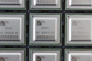
Figure 1 EPAC test samples
Initial bring-up was successful and EPAC executed its first bare metal program sending the traditional “Hello World!” greetings in different languages to EPI consortia and the world!
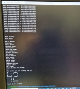
Figure 2 Hello World! screenshot
The outlook
EPI will continue to develop, optimize and validate different IP blocks and demonstrate features and performance of those thus creating an EU HPC IP ecosystem and make it available to the processor and accelerator industry and academia to create globally competitive production class building blocks for the next generation HPC systems.
The Initiative has successfully released EPAC1.0 Test Chip for fabrication
The European Processor Initiative (EPI) https://www.european-processor-initiative.eu/, a project with 28 partners from 10 European countries, with the goal of helping the EU achieve independence in HPC chip technologies and HPC infrastructure, is proud to announce that we have successfully released our EPAC1.0 Test Chip for fabrication.
One key segment of EPI activities is to develop and demonstrate fully European-grown processor IPs based on the RISC-V Instruction Set Architecture, providing power-efficient and high-throughput accelerator cores named EPAC (European Processor Accelerators). Using the RISC-V Instruction Set Architecture will allow leveraging open-source resources at hardware architecture and software level, as well as ensure independence from non-European patented computing technologies.
EPAC combines several accelerator technologies specialized for different application areas. The test chip, shown in figure 1 below, contains four vector processing micro-tiles (VPU) composed of an Avispado RISC-V core designed by SemiDynamics and a vector processing unit designed by Barcelona Supercomputing Center and the University of Zagreb. Each tile also contains a Home Node and L2 cache, designed respectively by Chalmers and FORTH, that provide a coherent view of the memory subsystem. The Stencil and Tensor accelerator (STX) was designed by Fraunhofer IIS, ITWM and ETH Zürich, and the variable precision processor (VRP) by CEA LIST. These specialized accelerators are connected with very high-speed network on chip and SERDES technology from EXTOLL.
The EPAC design was finalized by Fraunhofer IIS for chip integration in GLOBALFOUNDRIES 22FDX low-power technology and will be integrated and evaluated in the FPGA-based board designed by FORTH, E4 and the University of Zagreb. The successful fabrication of EPAC will showcase the next step in accelerator-based green HPC computing.
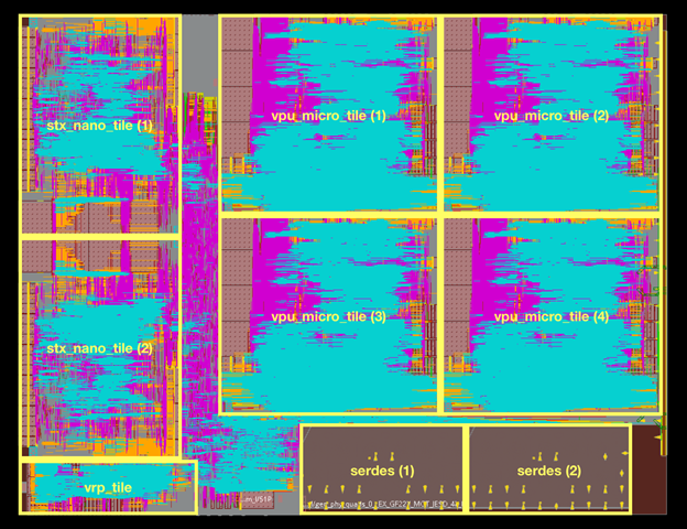
Figure 1 EPAC layout with VPU, STX and VRP accelerators with 25 mm2 in GF 22FDX technology
The outlook
The next generation of the EPAC accelerators and interfaces will be improved and refined for even higher performance and lower power levels in 12 nm technologies and below, and by adding a chiplet approach.
Jesus Labarta, BSC (EPAC Coordinator): I am really happy how partners with different backgrounds and motivations have been able to collaboratively develop this chip, putting all their efforts towards a collective success. It is a fully European design, driven by a vision of throughput-oriented computing and featuring characteristic that will result in high programmer productivity and achieve very high performance at low power and cost. Although just an initial Test Chip, it can be a significant step forward in HPC but also for edge and embedded applications.
Norbert Schuhmann, Fraunhofer IIS: The key challenge in this design and architecture was not only to achieve highest throughput and low power levels within the accelerators running on more than 1 GHz, but also to be in sync like in a concerto with memory accesses and data transport inside the chip and to the peripherals at rates above 200 Gbit/s.
The European Processor Initiative (EPI) https://www.european-processor-initiative.eu/, a project with 28 partners from 10 European countries, with the goal of helping the EU achieve independence in HPC technologies is proud to announce that we have successfully booted Linux on our EPAC 1.0 core subset implemented on FPGA.
One key segment of EPI activities is to develop and demonstrate fully European processor IPs based on the RISC-V Instruction Set Architecture, providing power efficient and high throughput accelerator core named EPAC (European Processor Accelerator). Using RISC-V will allow leveraging open-source resources at hardware architecture level and software level, as well as ensuring independence from non-European patented computing technologies.
First silicon implementation of EPAC 1.0 test chip is expected in the second half of 2021 and as an important technical milestone towards that goal, we have successfully booted Linux on a subset of EPAC 1.0 synthesized on FPGA. The FPGA design includes the Avispado RISC-V core, the Vector Processing Unit (VPU), the Network on Chip (NoC), the Shared L2 Cache with Coherence Home Node (L2HN), interrupt controllers, IO peripherals and several other components. This implementation will enormously speed-up software development on the EPI HPC architecture as well as testing and improving the architecture for next generations EPAC chips.
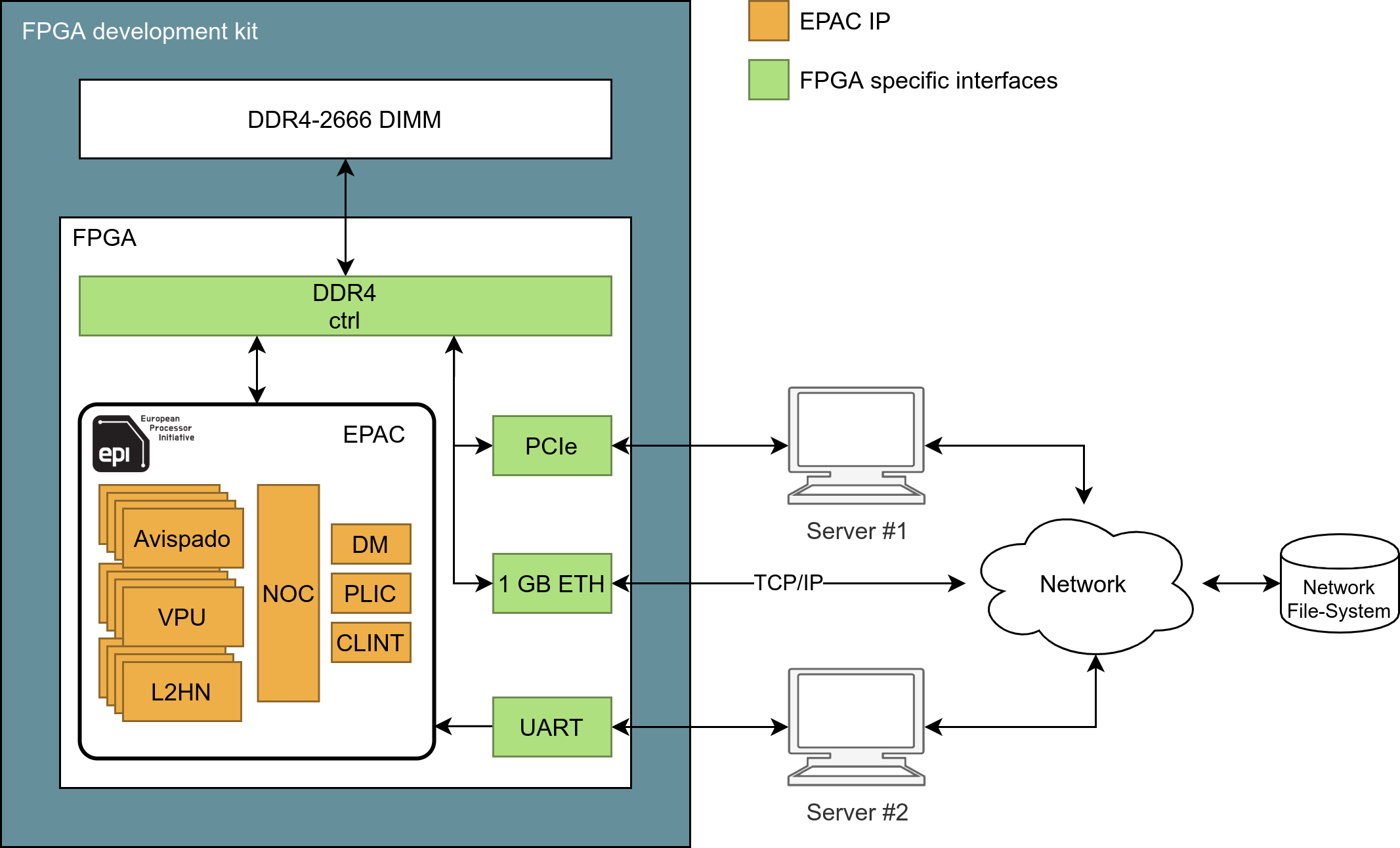
Figure 1 FPGA emulation and EPAC Software Development Vehicle block diagram
For the development of the EPI Accelerator Test Chip, we make extensive use of FPGA technologies to verify the RTL design of the Test Chip. The subset of EPAC 1.0 emulated on FPGA we use as Software Development Vehicle (SDV) to enable early software development before the actual Test Chip silicon comes back from the foundry.
The use of FPGAs enables the testing of RTL blocks with real and very complex software in timescales that are not tractable using pure RTL simulation. Also, it allowed us to stress memory coherence and several related corner cases. We have managed to boot Linux using the EPAC 1.0 system on FPGA and the system boots within a few dozens of seconds compared to weeks using pure simulation. The system is fully usable and interactive for system software and application development and it also includes Ethernet connectivity to enable running large and complex software packages, e.g., OpenMP, MPI.
This is a serious proof of concept that gives us the confidence of a functional and viable future product.
More details on the results can also be found on EPI YouTube Channel, where you can find the second episode of EPI Talks podcast, themed with booting Linux:
Channel: https://www.youtube.com/c/EuropeanProcessorInitiative/featured
Video: https://www.youtube.com/watch?v=X4klPnBjstI
The European Processor Initiative, a project with 27 partners from 10 European countries, with the goal of helping the EU achieve independence in HPC technologies, is finishing its second year of activities.
Despite 2020 bringing upon our young efforts the circumstances that were previously unimaginable, causing the subsequent cancellation of the first-ever planned European Processor Initiative Forum, the partners in the Initiative managed to stay the course and maintain all activities in all designated streams.
The year began with our latest partner, SiPearl, launching to start their activities dedicated to developing commercialized implementations of our technology. Very soon after announcing their presence on the global stage, SiPearl signed a licensing agreement with Arm and opened a branch in Germany.
At the same time, European Processor Initiative partners have finalized the first version of our RISC-V accelerator architecture, named EPAC, and we look forward to the delivery of the first European Processor Initiative silicon featuring EPAC Test Chip in the exciting year that follows. The EPAC Test Chip silicon will be complemented with PCIe EPAC Test Platform enabling the test and enhancements of the architecture for future revisions.
At the software level, we already have a compiler supporting RISC-V vector intrinsics and automatic parallelization of C/C++ codes. We are evaluating the generated code on emulation platforms that provide detailed insight for the holistic co-design of applications, compiler, and architecture. We also have other software development vehicles (SDV) where we are adapting the Operating System for the Heterogeneous ARM+RISC-V architecture of the European Processor Initiative project.
Our automotive activities in the previous year have been focused on the design of state-of-the-art automotive high-performance computing proof-of-concept with the ambition to demonstrate how European Processor Initiative IP will enable future ADAS functionality, paving the way to exploit the GPP, the RISC-V platform, the Kalray MPPA, and the Menta eFPGA IP.
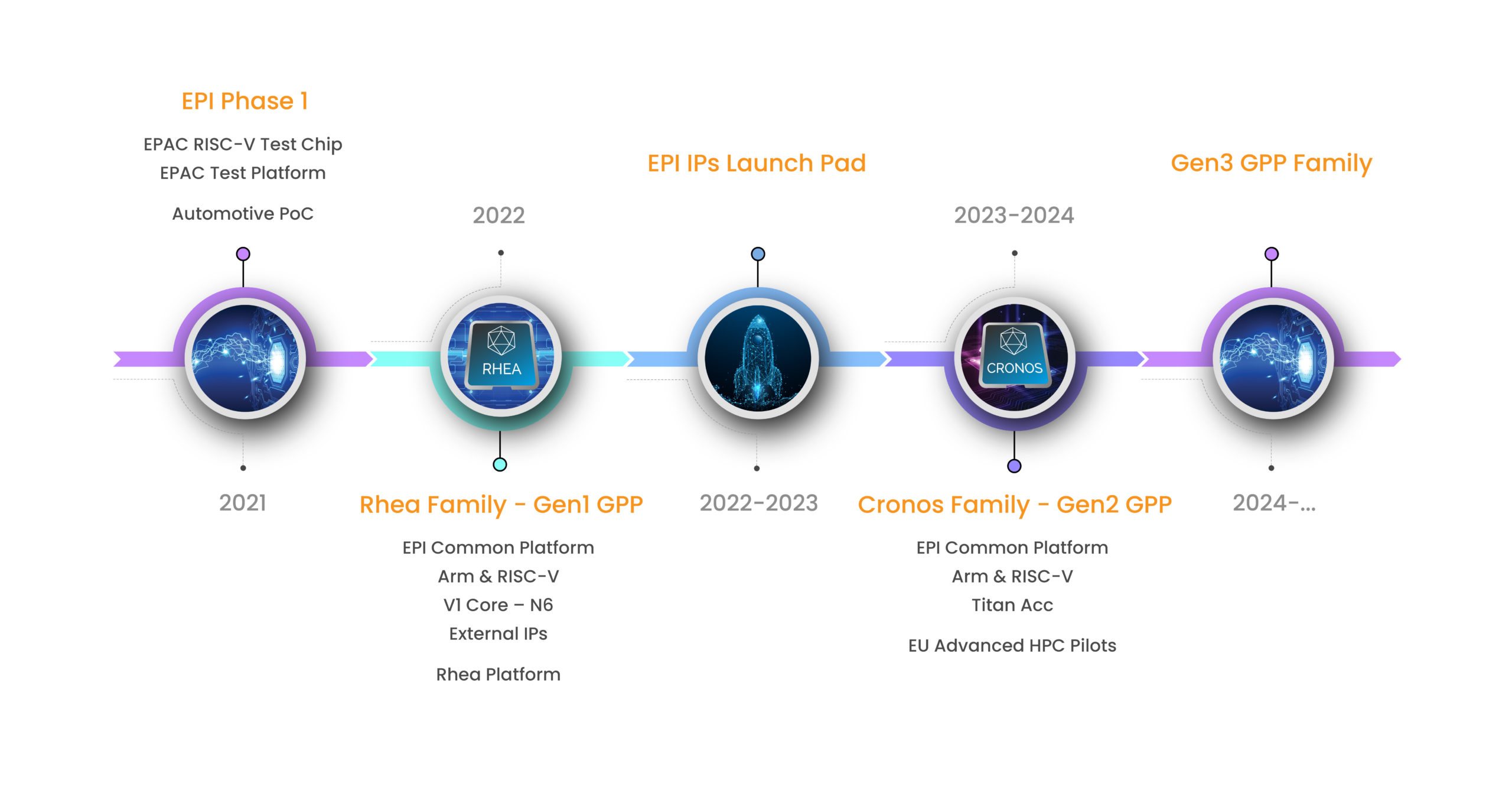
Based on this project progress, the Consortium is ready to announce the updated project roadmap shown below:
European Processor Initiative will, together with colleagues from other European exascale projects, attend the virtual Supercomputing20, where we will showcase our latest developments and update to the roadmap. We invite you to attend our virtual booth and join in the lively discussions about the future of HPC!